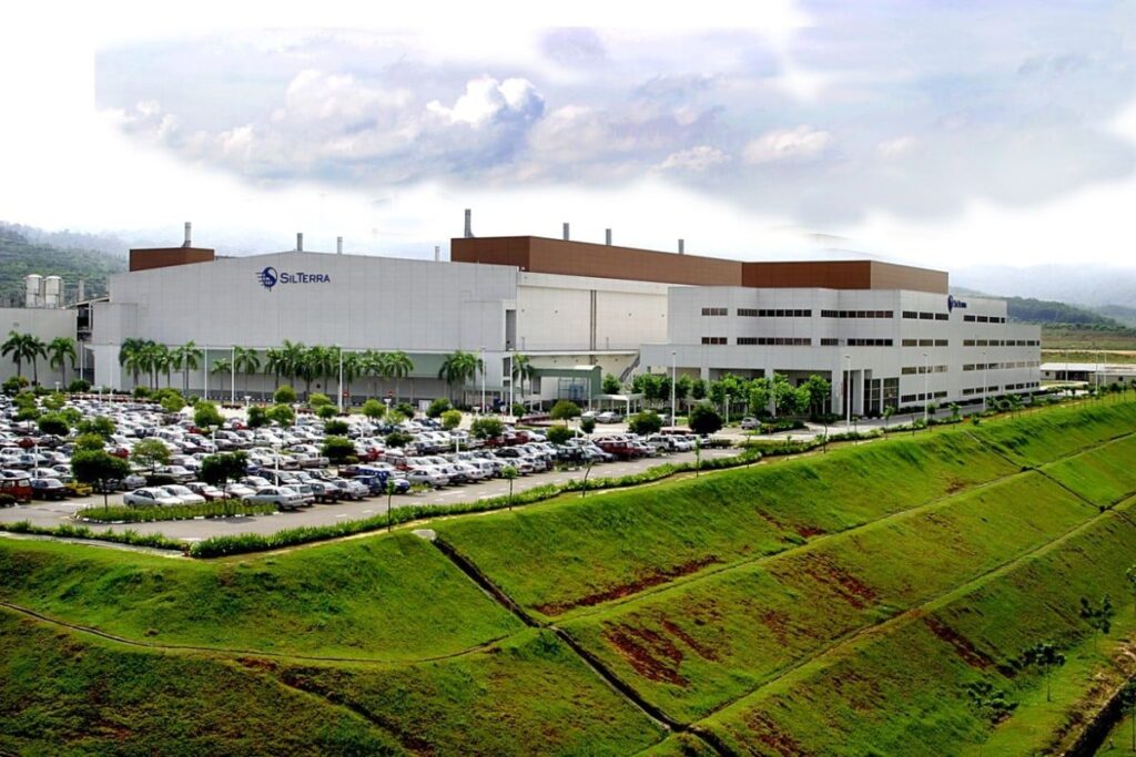
SilTerra, A Malaysia CMOS Foundry, Spearheading Malaysia’s Lone Effort in Silicon Photonics
SilTerra vice-president of strategic management Tan Eng Tong tells Digital Edge that it is moving full speed ahead and developing cutting-edge technology (alongside some of the leading R&D organizations in the world) such as silicon photonics, micro-electromechanical systems (MEMS), Internet of Things (IoT) and life sciences/biosciences applications and a state-of-the-art Covid-19 test kit to capitalize on what it sees as future demand
Since 2014, SilTerra has been working with Belgium-based Interuniversity Microelectronics Centre (IMEC) — a renowned international R&D organization active in the fields of nanoelectronics and digital technologies — to develop its own more cohesive and streamlined process to manufacture silicon photonics chips that have a major advantage over the conventional ones in the market.
This is an important factor, as the killer app for these silicon photonics chips is for use in data centers, the energy guzzlers of our time, consuming an estimated 1% of all the energy generated in the world for cooling processes. And with the introduction of cloud computing, more complex functions such as artificial intelligence and virtual reality, and 5G and autonomous vehicles later on, the situation is only going to get worse.
The problem now is how to reduce the heat generated by these data centers without breaking the bank. Tan says SilTerra was able to come up with its process technology because, unlike every other fab, it was not flush with funds, building new fabs, or trying to maximize return on investment.
He explains, “When you’re making money, you have the funds to invest in more factories and you want to load up these factories with high-volume jobs. We never got the funds to build more factories and do more stuff. So, our thinking process was that we would have to innovate without funds or be left far behind.”
The issue with funds is that you can only put it into things that guarantee volume, says Tan. “When you have funds, your stakeholders will ask when you are going to turn a profit. In the next six months? A year? And can you do it faster?”
Here is the problem with that. Anything new or innovative is necessarily low volume, at least to begin with. “So, when companies with these innovations go to these foundries, they are almost always turned away because they cannot order in high enough volumes,” he points out.
Tan says that, in nearly every case, the companies that approached SilTerra with innovative technologies had gone to one of the big boys first and were turned down. “We happen to be in the position where we have the capabilities and we have been working with other customers who are doing these technologies. Silicon photonics is just one of the things we are working on, but it’s the technology that happens to be the furthest ahead.”
He says those who have invested in this technology are planning three years because that is how long it takes technology to mature. “Tech is not the same as fashion. When fashion is hot, you buy it now. When technology is hot, you have to decide how long it will take to mature.”
IMEC approached SilTerra in 2014 with development work on optical waveguides. “We did not know at the time where it would lead to and considered this as assisting a research partner. Over time, this evolved, our capabilities improved and the market matured to what it is today,” says Tan.
He favours the “kueh lapis” (layered cake) analogy when describing the manufacturing process. “It involves stacking layers of silicon the depth of a fraction of a micron (a micron is one-thousandth of 1mm). A chip cannot be made as a simple piece; it needs to be made into a single tray called a silicon wafer, and then cut into pieces.”
This is very much like kueh lapis, says Tan. “The layers of silicon need to be layered one at a time and each layer needs to be cured before the next layer can be applied. In some chips, this can be as many as 24 layers, with each layer taking two to three days to complete, with additional processing steps in between.”
Each layer in the wafer is only a few hundred nanometres thick. “This requires some incredibly accurate machine tools, costing millions of dollars, depositing layers by the atom. But, unlike the kueh lapis, the chips are not flat. There are 3D structures that also have to be constructed, making channels and tracks to conduct electrons,” he says.
Silicon photonics chips are made of silicon but conduct photons instead of electrons, says Tan. “Their structures need to be adapted for guiding photons, also known as waveguides, very much like how a fiber-optic cable transmits light. Combining waveguides with semiconductors on the same wafer is the capability we have developed.”
As mentioned before, this is an incredibly difficult process and word got around that SilTerra was one of the few, if not the only one, that could do this. Lux Photonics Consortium program director Dr. Soo Choi Pheng says, “Silicon photonics uses light to move huge amounts of data at very high speeds, and SilTerra provides the right facility to support IC (integrated chip) product designers in realizing their innovation to make this not only faster but also propagate to a wider range of applications.”
Then, customers started to come a-calling. “The killer app, as I said, is still data centers, but some are looking to use it for optical networking (a communications system that uses light signals instead of electronic ones to send information between two or more points),” says Tan.
Here is how it works. “The customer, such as Nokia, works with us to develop chips for its applications and we manufacture these for the company. We also partner with companies such as Packaging Technologies GmBH (PacTech), which has been appointed by these customers to package the chips into modules to sell to network companies such as Nokia, which, in turn, market them to data center companies. Obviously, in the early stages of the market, only the biggest ones can afford them.”
Nokia’s chief technology officer for optical subsystems Michael Hochberg says working with SilTerra for the past several years has been a positive experience for the company. “We’ve been extremely impressed with their capabilities in terms of repeatability and process control, and their relentless focus on customer success. When we started working with them, we were a very young company and we needed to focus on building up a process where we could build highly differentiated silicon photonic chips.
“Since then, we’ve built parts for both telecommunications and intra-data center applications at speeds of 400G and beyond. I’ve developed processes in many fabs over the years and I’m consistently impressed by the SilTerra team’s responsiveness and eagerness to help.”
PacTech technical marketing manager Sim Sy Jiun is similarly impressed. “Our wafer-level packaging technologies complement its advanced technology areas of radio frequency, silicon photonics, MEMS and high voltage applications as an extension towards the middle and back-end of the supply chain. And we share a similar approach to providing high customization of advanced technologies in niche markets,” she says.
“SilTerra provided great support when we started our Malaysian subsidiary in Bayan Lepas, Penang, in 2008 and since then, we have been cooperating closely to strengthen the semiconductor ecosystem in Malaysia and Southeast Asia.”

Sometimes, customers come up with a design or product that requires the company to acquire new tools or equipment. In most cases, rather than making the huge investment needed, SilTerra has been able to persuade its customers to buy the equipment and place it in its fab for its use.
“Over time, they gradually transfer the equipment to us. We pay for it by giving them discounts on their wafers,” says Tan.
How much has SilTerra invested in silicon photonics? Tan is reluctant to assign a figure to it. “We didn’t buy any of the equipment specifically to develop silicon photonics. The equipment had already been around for 10 years when Khazanah invested in it and we gradually started using it for our other work,” he says.
“Our engineers kept trying different things and then they managed to come up with the innovation process to create embedded waveguides in the silicon photonics chips. So, the investment was mostly in the resources and the thinking process behind it.”
Now that it has been developed and has started to attract attention from end customers, what kind of returns is SilTerra projecting from silicon photonics alone? “We hope this new business will bring in US$45 million to US$60 million in revenue by 2023. Of course, we hope it will grow even further from that point,” says SilTerra CEO Firdaus Abdullah.
Tan says the company is already shipping out silicon photonics chips, but it is not very visible at the moment. “The big growth is going to be in 2022 and 2023. These things are not like smartphone innovations, which show up in six months.
“There are certain cycles that a data center has to go through. First, they have to qualify the material and then, they have to put it in their budgets for the year after. And the year after that, they will migrate to it in the thousands. Once the big boys start using it, the others will follow.
“Last year was the start of the qualification period, which means they will all be using these chips for six months or so to see whether there is an appreciable savings in energy. Once they are happy with it, they will start planning and budgeting to implement this new technology. Then, we should start to see the numbers coming in. The potential is mind-blowing.”
Reposted from: https://theedgemalaysia.com/article/cover-story-silterra-surges-ahead-silicon-photonics
